Fixing DRC Errors
Written by Person20020/Koji
When designing a PCB, it is inevitable that you will have some issues on your first try. KiCad has integrated tools to check your design to catch some of the most common errors. These tools are the Electrical Rules Checker (ERC) for the schematic and the Design Rules Checker (DRC) for the PCB.
This guide will go over some of the most common ERC/DRC errors and how to fix them.
I will include a quick explanation and summary of what you need to do to fix it (or if it can be ignored) in bold text and for some errors there will be a longer explanation of what the issue is in italic text.
Run DRC/ERC
Section titled “Run DRC/ERC”You can run DRC or ERC by clicking this button with a list icon in the top bar of the PCB or schematic editor respectively.
 Then click
 Run DRC/Run ERC. It will give you a list of issues that it finds. You can click on an issue to have KiCad center your screen on its location. When you are done you can get rid of all of the arrows by clicking Delete All Markers.
Errors vs Warnings
Section titled “Errors vs Warnings”ERC and DRC categorize the issues they find into two groups, errors and warnings.
Errors are large issues that KiCad thinks could cause your PCB to not function properly. This includes things like not having enough clearance from a trace to the edge of your board, which could result in it being damaged when the outline of the board is milled.
Warnings are smaller issues that probably won’t prevent the board from functioning, but may affect the appearance of your pcb. This could include your silkscreen being cut off or being too small to read. Some warnings can include issues affecting the functionality of the design, but these generally will be smaller issues, or ones that KiCad is not fully sure are actually a problem.
ERC (Schematic)
Section titled “ERC (Schematic)”ERC checks for issues in your schematic. It won’t be able to catch things that are fundamentally wrong with the design (things like connecting 5v to a component that needs 3.3v), but it can tell you things like if you forgot connect a pin.
ERC can often be triggered by things such as symbols that were designed incorrectly with the wrong pin electrical type and some of them can be ignored, but before you do so you should at least understand what it is saying so you know if this is actually the case.
Most ERC warnings (along with many ERC errors) should be pretty self explanatory. Most of them are basically ‘Something is connected that shouldn’t be’ or ‘Something that should be connected isn’t’. If you think something should be here, DM me (@Person20020)!
Input pin not driven by any Output pins or
Section titled “Input pin not driven by any Output pins or”Input Power pin not driven by any Output Power pins
Section titled “Input Power pin not driven by any Output Power pins”This is usually caused by a symbol that didn’t properly assign the pin electrical types. It can generally be ignored. If there is nothing connected to the pin, this can be solved by adding a No Connect Flag.
The pin electrical types describe what a pin does and allows KiCad try to see if you connected the wrong types of pins together, e.g. to check if you connected two 5v pins together, but both are expecting an input rather than one being an output which supplies the other with power.
Pin not connected
Section titled “Pin not connected”When a pin is not connected to anything, it should be indicated that this is intentional by using No Connect Flags. This will stop the error for the pin.
DRC (PCB)
Section titled “DRC (PCB)”DRC checks for issues in your PCB design. It is much more important to pay attention to these as they are do not give false positives nearly as often as ERC. Again, it is important to understand why you are allowed to ignore an error before you do so that you don’t miss something important.
Electrical
Section titled “Electrical”These are electrical issues with your design that include stuff like shorted traces, etc.
Items shorting two nets
Section titled “Items shorting two nets”Something is connecting two ‘nets’ that should not be connected. Find it and make it not connected.
Tracks crossing
Section titled “Tracks crossing”Traces are intersecting that shouldn’t be. Use vias to go around or fix it in some other way.
Clearance violation
Section titled “Clearance violation”Some pads/tracks are too close together. If this is coming from a footprint you can change your clearance rules in File->Board Setup->Design Rules/Constraints and set Minimum clearance to 0.1mm (the JLCPCB minimum). Otherwise you can move the things causing the error apart.
Via is not connected or connected on only one layer
Section titled “Via is not connected or connected on only one layer”A via isn’t fully connected. Find it and connect or delete it.
Track has unconnected end
Section titled “Track has unconnected end”There is a trace with one end left unconnected. Find it and connect it if needed, otherwise delete it.
Thermal relief connection to zone incomplete
Section titled “Thermal relief connection to zone incomplete”There is a pin connecting to a fill zone that does not have the minimum required number of connections. If there is space around the pin, move traces or other things out of the way to give room. If there will not be a large amount of power going through this (such as for Hackpad), you will most likely be fine to decrease the minimum number to one. You can do this in File->Board Setup->Design Rules/Constraints in the Minimum thermal relief spoke count setting.
Design for Manufacturing
Section titled “Design for Manufacturing”These are issues that affect how your PCB will be manufactured. If they are not fixed, JLCPCB may reject it or it could cause issues with the PCB.
You can look at these manufacturing capabilities from JLCPCB to make sure you have enough clearance.
Board edge clearance violation
Section titled “Board edge clearance violation”Something is too close to the edge of your PCB. This can be either at the outer edge of the PCB or near a cutout (including those in footprints like the SK6812MINI-E). The default KiCad clearance rules give a lot of extra room and will be triggered by some footprints. JLCPCB allows a minimum of 0.2mm of clearance. You can change it in File->Board Setup->Design Rules/Constraints and set Copper to edge clearance.
Hole clearance violation
Section titled “Hole clearance violation”Something is too close to a hole. Move it away. You can also reduce Copper to hole clearance in File->Board Setup->Design Rules/Constraints to 0.2mm if needed.
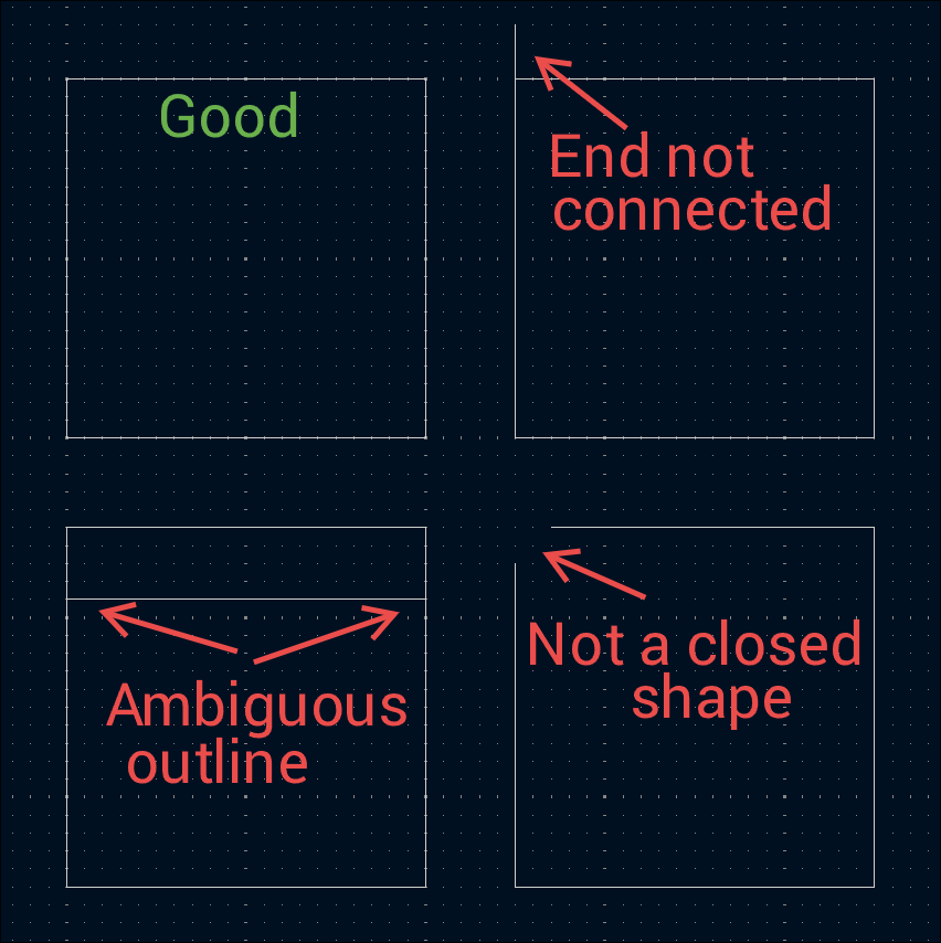
Board has malformed outline
Section titled “Board has malformed outline”The outline of the PCB (the Edge.Cuts) has a gap, part that sticks out with an unconnected end, or otherwise ambiguous outline. The outline must be one continuous loop.
Solder mask aperture bridges items with different nets
Section titled “Solder mask aperture bridges items with different nets”There is a hole in the solder mask that includes pads/pins/etc from different nets (a net is basically a groups of pins that are electrically connected together). This could lead to the pads being shorted when soldering as the solder mask is not there to repel the solder. There are some cases where this is intended, such as when making solderable jumper pads, however it is generally not good. This may happen if the footprint is designed badly and not all parts of a pad are assigned a pin number, in which case it can (ideally) be fixed by editing the footprint, or ignored.
YOU SHOULD UNDERSTAND WHAT THE ISSUE IS BEFORE IGNORING THIS!
Schematic Parity
Section titled “Schematic Parity”Something doesn’t match between your schematic and PCB. This should be fixed.
Missing connection between items
Section titled “Missing connection between items”Something isn’t connected… Connect it.
Readability
Section titled “Readability”All of these warnings pertain to the silkscreen, which although helpful, is purely cosmetic and may be ignored. You can (and should) fix them if you want to.
Silkscreen overlap
Section titled “Silkscreen overlap”Two or more silkscreen items are overlapping.
Silkscreen clipped by solder mask
Section titled “Silkscreen clipped by solder mask”An item on the silkscreen is cut off by a hole in the solder mask.
Silkscreen clipped by board edge
Section titled “Silkscreen clipped by board edge”An item on the silkscreen is cut off by the edge of/a hole in the PCB.
To fix any of the above, just move the silkscreen.
Text height out of range or
Section titled “Text height out of range or”Text thickness out of range
Section titled “Text thickness out of range”Some text on the silkscreen is very small or thin and may be hard to read. If you want to fix this you can select the text, right click->Properties… and increase the Width and Height or Thickness.
Mirrored text on front layer or
Section titled “Mirrored text on front layer or”Non-Mirrored text on back layer
Section titled “Non-Mirrored text on back layer”Some text may be backwards. If so, select it, Right click->Properties...->click the mirror button on the right.

Miscellaneous
Section titled “Miscellaneous”Text (or dimension) on Edge.Cuts layer
Section titled “Text (or dimension) on Edge.Cuts layer”There is some text (or dimensions) on the Edge.Cuts layer. these things should most likely be on the F.Silkscreen/B.Silkscreen layers. You can change it by selecting the object, Right click->Properties... and then change the Layer to F.Silkscreen for the front of the PCB or B.Silkscreen for the back.
Isolated copper fill
Section titled “Isolated copper fill”You have a filled zone with isolated sections that are not connected to anything. You can either connect it to the rest of the zone or select the zone and Right click->Properties... and set Remove islands to Always.
Footprint doesn’t match copy in library
Section titled “Footprint doesn’t match copy in library”If you edited the footprint this can happen. Select the footprint, then Right click->Update Footprint... then click Update.

These Words Mean Stuff
Section titled “These Words Mean Stuff”A quick explanation of some terms I use on this page.
Net
A 'net' is basically a 'group' of all things that will all be electrically connected together. E.g. the GND net will connect to all GND pins and the 5V net connects to all of the 5V pins on your PCB.Silkscreen
Silkscreen is the layer on the PCB used to show graphics. It is often used to show the outline of parts and indicate the direction in which it should be soldered. It can also include text or any other thing you want to print on the PCB for information/decoration. In KiCad this is on the F.Silkscreen/B.Silkscreen layers.Solder Mask
Solder mask is another layer on the PCB which repels solder. It covers all of the board except for the pads to prevent solder from spreading and bridging multiple pins. In KiCad this is the F.Mask/B.Mask layers.Thermal Relief Connection
When a pin is connected to a zone, it is not connected all around the pin. It instead uses several 'spokes' to prevent heat from being sucked away as quickly when soldering.If you come across any others that I have missed, you can DM me in slack @Person20020!